Channels
Special Offers & Promotions
Institute for Factory Automation and Production Systems Installs TESCAN AMBER X Plasma FIB-SEM for Diverse Set of Materials Research Projects

APS will use the FIB-SEM for silver printing and copper coating analysis in an effort to improve mechatronic systems, battery components, additive manufacturing and more
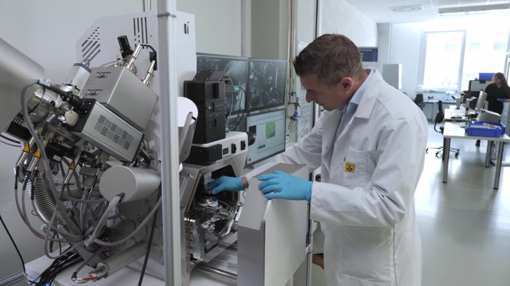
TESCAN ORSAY HOLDING a.s. announces the installation of the AMBER X focused ion beam-scanning electron microscope (FIB-SEM) at the Institute for Factory Automation and Production Systems (FAPS) in Germany. The AMBER X offers a unique combination of plasma FIB with ultra-high resolution (UHR) field emission SEM for multiscale materials characterization. FAPS is using the FIB-SEM for research that will help to improve products used in a wide variety of industries, including automotive, printed electronics, battery and additive manufacturing, renewable energy and medical technology.
“When we purchased our FIB-SEM, we were looking for a robust instrument with a high level of flexibility so that we could use it for characterization on a wide range of materials,” said Martin Muckelbauer, Research Engineer at FAPS. “We have research coming in mostly from industry that involve large sample areas, but we also need to capture tiny, precise details with high resolution and magnification. Hence, the sample versatility and UHR imaging capabilities of the AMBER X, together with high throughput, was very important to us.”
FAPS is studying silver printing technology to improve the reliability of electronic components used in a diverse range of consumer products. They are using the AMBER X for three-dimensional (3D) failure analysis and characterization to look at delamination, cracking, hotspots and porosity.
Research involving copper coating technology focuses on improving electrical conductivity in order to eliminate oxides and pores from structures. This work will help to improve inverter and battery technology and additive manufacturing. The AMBER X is ideal for this application due to its high-throughput capabilities for cutting through layers of material and ability to provide high-resolution details of the sample surface and melted particles.
According to Martin Sláma, TESCAN’s Product Marketing Manager for FIB-SEM 3D characterization and TEM lamella preparation in materials science, “FAPS is helping to improve the world by pushing the boundaries in electronics research. They were looking for a versatile instrument that can support a wide range of materials for their busy lab. The AMBER X met their needs for flexibility, robustness, and capability to analyze large areas easily.”
TESCAN enables nanoscale investigation and analysis within the geosciences, materials science, life sciences and semiconductor industries. The company has a 30-year history of developing innovative electron microscopy, micro-computed tomography, and related software solutions for customers in research and industry worldwide. As a result, TESCAN has earned a leading position in micro- and nanotechnology.
TESCAN ORSAY HOLDING was established in 2013 as a result of long-term expansion and establishment of subsidiaries worldwide, including France-based ORSAY PHYSICS, a world leader in customized focused ion and electron beam technology. TESCAN ORSAY HOLDING maintains its headquarters, production and R&D in Brno, Czech Republic. Every TESCAN microscope is expertly produced in Brno and shipped to customers worldwide.
About the Institute for Factory Automation and Production Systems
The FAPS institute was founded in 1982. Its overarching objective is the integration of all the manufacturing factory functions for a comprehensive computer-integrated concept. Prof. Franke established the focus of research to be on innovative and interdisciplinary manufacturing process approaches to mechatronics products.
Research conducted at the institute encompasses the entire process chain for mechatronics products that begins with packaging electronic components, with the main focus on the assembly of electronic components (solder-printing, assembly, soldering, testing), and the production process of electrical drives (winding methods, joining techniques, magnet mounting). Also, the research focus considers the methods and equipment involved in development, along with the assembly of connecting and embedding the cable systems.
The institute is located at two sites. The first is at the FAU’s Technical Faculty campus in Erlangen, and the second is at the former industrial sites of AEG in Nuremberg. The chair currently has about 110 employees from interdisciplinary research fields in mechanical engineering, electronics engineering, computer sciences, mechatronics, mathematics and engineering management. The institute research factory is about 2,500 m2 accomodating high-capacity machines and equipment for the manufacturing of mechatronics products. The quality of the mechatronics components and systems can be assessed by the existing test systems for climate, temperature changes and vibration models. Modern EDV systems facilitate computer-aided design and the simulation of products and processes.
The FAPS institute is also involved in teaching activities for support of the Department of Mechanical engineering. The education and training is strongly reinforced through the modern test facilities for component manufacturing, assembly and electronics manufacturing.
Media Partners


