
Channels
Special Offers & Promotions
Unlocking Materials 4.0
Harnessing always-on, data driven results
A rise in Industry 4.0 technologies emphasizes instantaneous access to data for better-informed decision-making. While this is most commonly seen in manufacturing, many other 'point four' paradigms are embracing the need for always-on, data-driven results. Here, Franz Kamutzki, Senior Sales Account Manager at specialist in electron microscopy for industrial materials, Thermo Fisher Scientific, explains the concept of Materials 4.0 and how it addresses the complex needs of scientists in material characterization.
Materials 4.0 represents the convergence of advanced digital technologies with traditional materials science, ushering in a new era of efficiency in the discovery, development and deployment of materials. Inspired by the principles of Industry 4.0, this approach leverages big data, high-throughput experimentation and integrated computational tools to reimagine how materials are designed and used.
For instance, an advanced microscope could autonomously analyze and classify material microstructures, while instantly sharing data through a cloud-based platform. This eliminates the need for repetitive, manual data input tasks, and enables continuous refinement of material designs, significantly accelerating research and improving the precision and scalability of material innovations.
The challenge of becoming data driven
While this sounds promising, bringing Materials 4.0 to fruition is not without its challenges. In materials research and development labs, initiating such projects can be difficult and expensive. Research from the Henry Royce Institute and the University of Liverpool illustrates this well, noting: "Current approaches to lab automation in chemistry have tended to focus on the development of large highly integrated platforms... requiring substantial capital investments and specialized teams for management and maintenance”.
Implementing Materials 4.0 in the context of microscopy often requires additional IT infrastructure that’s capable of handling, and extracting value from, the data generated by modern electron microscopes. Additionally, staff may require extensive training to effectively use these new tools, and scaling these technologies across different departments or locations can be challenging, especially if existing infrastructure and processes are not standardized.
To bring advanced analytics to materials science, new technologies need to be able to integrate into existing set ups with ease and without adding any extra complexity. A good microscopy system that’s ready for Materials 4.0 should also streamline data management, eliminating the need to juggle multiple sources. But what could this look like?
Scanning electron microscopy and Materials 4.0
Scanning electron microscopy (SEM) is a vital technology for data-driven material science — particularly for the characterization and analysis of materials. The high-quality, high-resolution data generated by SEM can be integrated with machine learning algorithms to automate the analysis of complex microstructures, identify defects and predict material properties. This automated approach significantly enhances the efficiency of the materials discovery process, allowing for the rapid screening and optimization of new materials.
Today’s SEMs are a world apart from those used almost 100 years ago. Technologies such as electron Backscatter Diffraction (EBSD) make it possible to analyze the crystallographic orientation and phase distribution of materials at the microstructural level. By detecting and analyzing diffraction patterns from backscattered electrons, EBSD provides detailed maps of grain orientation, phase identification, and strain distribution. This high-resolution, quantitative data is crucial in the context of Materials 4.0.
Consider the study of solid-state batteries. Researchers can monitor the behaviour of the generally crystalline cathode materials using EBSD. This technique allows them to investigate texture, grain size, and boundary distributions, all of which are anticipated to be connected to the electrochemical performance of the cathode material and, consequently, the battery.
A new approach to SEM
To realize Materials 4.0, advanced analytics are often thought to require multiple pieces of equipment and software. However, the right SEM can streamline this process by integrating essential features into a single platform.
A suitable SEM for Materials 4.0 must offer ultra-high resolution to accurately examine surface features such as grain boundaries and defects. It should also seamlessly integrate with lab automation tools and advanced analytical techniques like Energy Dispersive X-ray Spectroscopy (EDS) and EBSD to simplify data acquisition and reduce reliance on multiple systems. In the example of lithium-ion batteries, combining EDS with SEM could allow researchers to obtain both high-resolution images and chemical composition data simultaneously. This means that, while observing the formation of lithium dendrites in real-time, researchers could also analyze the chemical composition of these dendrites as they form.
An SEM that incorporates these technologies directly into its platform simplifies the analysis workflow by eliminating the need for separate instruments. This integration allows engineers and materials scientists to acquire comprehensive data — both visual and compositional — in a single setup. It streamlines data acquisition, enhances the accuracy of the analysis and reduces the complexity of managing multiple systems. As a result, engineers can more efficiently assess the quality and performance of the material, leading to improved reliability and optimized final products.
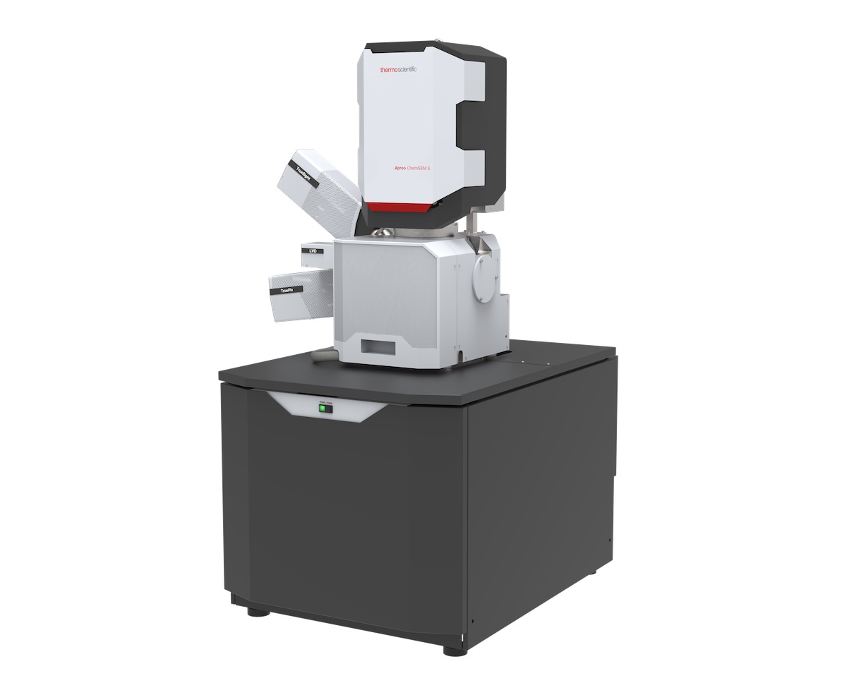
Thermo Fisher Scientific’s answer to the requirements of Materials 4.0 is its ChemiSEM technology. An advanced feature in SEMs, ChemiSEM combines traditional SEM imaging with elemental analysis in real-time. It allows users to see the chemical composition of a sample directly within the SEM image, without needing to switch to a separate EDS system. This integration makes it faster and easier to obtain both visual and compositional information simultaneously, enhancing productivity and reducing the complexity of sample analysis.
Now, the company is launching the technology on its Thermo Scientific™ Apreo™ SEM. With a first of its kind integration of SEM, EDS and EBSD analytics, the Apreo ChemiSEM™ removes the barriers that having multiple component and software interfaces often bring to SEM. Instead, users can acquire, store, share and analyze material data through a single platform. Where performing EBSD once required a specially trained operator, the Apreo ChemiSEM makes advanced materials analysis possible for all users. Additionally, as analytics are integrated into the SEM, service, support and sales advice all comes from a single point. This means users do not need to juggle multiple service operators and all support can be given from a single Thermo Fisher expert who can help users make the most out of their microscope.
As data-driven decision making takes rise across industry, materials analysis faces its own precipice of change. While automation in the laboratory has typically required an equipment overhaul and specialized expertise, access to integrable, user-friendly analytics is enabling the sector’s own “point four” shift. Electron microscopy will remain fundamental in the characterization and analysis of materials and, when enabled with the latest SEM technology, we’ll see Materials 4.0 truly come to fruition.
About Thermo Fisher Scientific
We are the world leader in serving science. Our Mission is to enable our customers to make the world healthier, cleaner and safer. Our innovative solutions for electron microscopy, surface analysis, and microanalysis help materials science researchers advance their sample characterization to gain deeper insight into the physical and chemical properties of materials from the macroscale to the nanoscale. Our multiscale, multimodal solutions cover a broad range of applications across dozens of industries and research fields, serving customers in academia, government, and industry. Our TEMs, DualBeam™ FIB-SEMs, comprehensive portfolio of SEMs, XPS, and microanalysis solutions, combined with software suites, take customers from questions to usable data by combining highresolution imaging with physical, chemical, elemental, mechanical, and electrical analysis across scales and modes.
Recent news from Thermo Fisher Scientific
News Channels
- Latest News
- New Laboratory Products
- Industry News
- Laboratory Automation | IT Solutions
- Microscopy | Image Analysis
- Separation Science
- Research | Case Studies
- Video Presentations
- Events | Conferences
Subscribe to any of our newsletters for the latest on new laboratory products, industry news, case studies and much more!
Popular this Month
Top 10 most popular articles this month
Today's Picks
Looking for a Supplier?
Search by company or by product
Please note Lab Bulletin does not sell, supply any of the products featured on this website. If you have an enquiry, please use the contact form below the article or company profile and we will send your request to the supplier so that they can contact you directly.
Lab Bulletin is published by newleaf marketing communications ltd.
Media Partners