Channels
Special Offers & Promotions
TESCAN Launches Next Generation AutoSlicer Module for High Throughput TEM Sample Preparation
TESCAN’s new AutoSlicer enables high quality samples to be prepared more quickly and consistently and with fewer artifacts
TESCAN ORSAY HOLDING a.s. announces its latest generation AutoSlicer™ module for unattended, semi-automated transmission electron microscope (TEM) lamella preparation in semiconductor failure analysis and materials science. For both Gallium (Ga) focused ion beam (FIB)-scanning electron microscope (SEM) and Plasma FIB-SEM instruments, TESCAN’s AutoSlicer enables high throughput TEM sample preparation at multiple sites or on multiple samples and provides full control over the specific parameters required for optimal sample quality.
Automating the initial TEM sample preparation process steps speeds processing time, assures sample uniformity, and alleviates concerns that samples may not meet the quality requirements for subsequent imaging and analysis. As the number of samples needing to be prepared daily increases, researchers and engineers need to improve sample preparation throughput even as the samples themselves are becoming more challenging to prepare because of smaller features and ever-shrinking device nodes.
“Plasma FIB is gaining ground as a technique for thin sample preparation, because Xe Plasma FIB-prepared lamellae are free of gallium implantation and have significantly less beam-induced surface damage,” states Jozef Vincenc Obo?a, product marketing director, Semiconductors at TESCAN. “By extending unattended sample preparation capabilities of AutoSlicer for TESCAN Ga FIB-SEM to our Xe plasma FIB-SEM instruments, we are able to help our users further leverage both the time-savings and sample quality advantages of Plasma FIB, with samples prepared more quickly, more consistently, with fewer artifacts and less amorphization.”
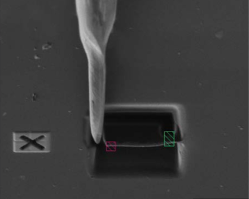
TESCAN AutoSlicer automates the initial steps in the TEM sample preparation workflow: navigation to regions of interest, protective layer deposition, trench milling, polishing and the undercut to release the sample from the trench. Following these initial preparation steps, AutoSlicer’s semi-automated workflows guide users through lift-out and attachment of the lamella to the TEM grid. Users can develop custom workflows unique to their samples which are then saved within AutoSlicer and recalled as needed. Also, like all TESCAN software modules, AutoSlicer is fully integrated within the TESCAN Essence user interface, so it is easy to understand and operate, even for users who don’t have extensive sample preparation experience.
TESCAN AutoSlicer also can be used to prepare multiple samples for electron backscatter diffraction (EBSD) or other analyses, or to automate FIB milling at multiple locations or on multiple samples. AutoSlicer is fully integrated within the TESCAN Essence user interface and is available for TESCAN AMBER and TESCAN SOLARIS Ga FIB-SEM instruments and for TESCAN AMBER X and TESCAN SOLARIS X Plasma FIB-SEM instruments.
About TESCAN
TESCAN enables nanoscale investigation and analysis within the geosciences, materials science, life sciences and semiconductor industries. The company has a 30-year history of developing innovative electron microscopy, micro-computed tomography, and related software solutions for customers in research and industry worldwide. As a result, TESCAN has earned a leading position in micro- and nanotechnology.
TESCAN ORSAY HOLDING was established in 2013 as a result of long-term expansion and establishment of subsidiaries worldwide, including France-based ORSAY PHYSICS, a world leader in customized focused ion and electron beam technology. TESCAN ORSAY HOLDING maintains its headquarters, production and R&D in Brno, Czech Republic. Every TESCAN microscope is expertly produced in Brno and shipped to customers worldwide.
Media Partners


