Channels
Special Offers & Promotions
European HITACHI-Workshop at Fraunhofer IMWS
The Fraunhofer Institute for Microstructure of Materials and Systems IMWS expands its range of microstructure diagnostics with Hitachi's HF5000 field emission transmission electron microscope.
The presentation of the new microscope took place during a workshop in Halle (Saale). In this meeting, international experts were presented with novel microscopy technologies as well as a demonstration of possible applications of the HF5000.
The workshop focused on new research possibilities that arise with the HITACHI HF5000 for nano and surface analysis. By means of an electron beam obtained from a cold field emission source and an electron-optical probe corrector, subangstrom beam diameters can be generated. This provides researchers with even more precise insights into the nanostructure of, for example, glasses, glass-ceramics and optical layers. As a result, microstructural defects can be more clearly recognized, element distributions can be mapped more easily, and work on improving material properties will be significantly accelerated.
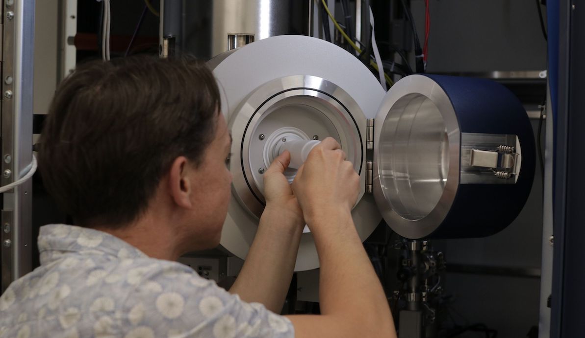
Global researchers and Hitachi experts spoke at the workshop about working with this cutting-edge microscopy technology. At Fraunhofer IMWS, the first HITACHI HF5000 in Europe was installed. Yasukuni Koga from Hitachi High-Technologies confirmed at the end of the workshop: "We are very pleased to have found a premium partner in Europe with the Fraunhofer IMWS, who fully utilizes the application possibilities of the HF5000. The workshop has confirmed that we can shape the future and expand technological boundaries through this great collaboration."
The microscope in Halle is mainly used by the recently founded business unit »Optical Materials and Technologies« of the Fraunhofer IMWS. Prof. Thomas Höche, Head of this business unit, is particularly pleased by this unique selling point. During his presentation he spoke about the added value of the new microscope for the institute and its customers. »I am proud that our team is the first in Europe to work with the HITACHI HF5000. We benefit from the outstanding quality of the element distribution mappings in particular as an applied research institution and thus the companies that we support in the improvement of their products. For example, we can identify microstructural vulnerabilities in materials used in the optical industry or the paint industry more quickly and offer solutions for avoiding them. Our business unit will not only characterize materials down to the atomic level, but also develop them." After the talk, attendees were given a tour to get to know the microscope, how it works, and the lab built specifically for the equipment.
The special feature of the high-resolution, analytical 200-keV scanning transmission electron microscope HF 5000, which combines the TEM and the STEM technology, is the significant increase in performance when acquiring STEM images. Due to the beam generation by means of cold field emission and the implemented probe corrector, the HF5000 can also be used for investigations with only 60 kV acceleration voltage. A special added value is provided by the detectors for excited X-ray radiation, which measure a spatial angle of 2.2 Steradians, which is three times the best TEM / STEM at Fraunhofer IMWS offer so far and contributes to the faster acquisition of elemental distribution images.
About the Fraunhofer Institute for Microstructure of Materials and Systems IMWS
The greatest challenge facing mankind in the 21st Century is the question of sustainability in all spheres of life, especially in the efficient use of limited raw materials. The Fraunhofer Institute for Microstructure of Materials and Systems IMWS conducts applied research in the field of material efficiency and is a major driving force, innovator and problem solver for the industry and public-service clients in the fields of reliability, safety, service life and functionality of materials used in components and systems. The key competences are to be found in the fields of characterization of materials down to the atomic scale and in material development.
About Hitachi High-Technologies Europe
Hitachi High-Technologies Europe offers a diverse product line-up from sample preparation to ultra-high resolution scanning electron microscopes (SEM). Hitachi High-Technologies systems include tabletop SEM systems that allow quick user-friendly operation, FE-SEM and TEM systems for performing precise detailed analysis, FIB-SEM systems that are capable of three-dimensional analysis, and AFM systems that allow the simultaneous measurements of surface topography.
News Channels
- Latest News
- New Laboratory Products
- Industry News
- Laboratory Automation | IT Solutions
- Microscopy | Image Analysis
- Separation Science
- Research | Case Studies
- Video Presentations
- Events | Conferences
Subscribe to any of our newsletters for the latest on new laboratory products, industry news, case studies and much more!
Popular this Month
Top 10 most popular articles this month
Today's Picks
Looking for a Supplier?
Search by company or by product
Please note Lab Bulletin does not sell, supply any of the products featured on this website. If you have an enquiry, please use the contact form below the article or company profile and we will send your request to the supplier so that they can contact you directly.
Lab Bulletin is published by newleaf marketing communications ltd.
Media Partners