Channels
Special Offers & Promotions
Queensgate launches new nanopositioning stages
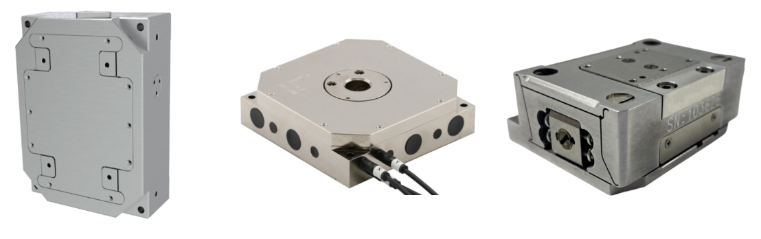
Queensgate piezo nanopositioning stages are available now for high-precision applications in microscopy, metrology, semiconductor manufacture, and industrial inspection.
The exciting new developments include:
- A heavy-duty single-axis stage with a 6 kg load capacity and sub-nanometer precision that is ideal for Z scanning.
- A multi-axis stage with flexure guidance that ensures minimal rotational errors (less than 25 micro-radians over the full travel range) for atomic force microscopy applications.
- A long-range 500 µm stage with market-leading resolution and accuracy for semiconductor and material inspection applications.
Heavy-duty single-axis stage for objective positioning & motorized nosepiece Z scanning
Queensgate’s NPS series high-load 250 μm piezo stage has been designed to precisely position loads of up to 6 kg. It is ideally suited to positioning optical nose-pieces and assemblies for non-contact metrology techniques such as white light interferometry (WLI) surface topography as well as other precision manufacturing or inspection tasks that require accurate positioning of heavy loads.
Ideal applications for this stage include optical nosepiece positioning, semiconductor inspection, white light surface metrology and precision manufacturing.
Multi-axis stage with flexure guidance that is ideal for atomic force microscopy
An evolution of Queensgate’s proven high-dynamic 100 µm XY stage, the NPS-XYZ-100D-20H adds a 20 µm of vertical travel which enables advanced AFM, SPM or other imaging techniques such as NSOM. The open aperture means it is also suitable for the precision alignment or scanning in optical systems.
Ideal applications for this stage include AFM, SPM, NSOM and high precision microscopy.
Ultra-compact long-range piezo stage for semiconductor & materials inspection
With a footprint of just 50 × 60 mm, the NPS-Z-500C is ideally suited for integration into complex systems where space is limited. Its moving platform remains flat throughout the full 500 µm range of travel, enabling cantilevered semiconductor probes or biological samples to be positioned at the edge of the stage while maintaining confidence in the motion profile.
Ideal applications for this stage include high precision microscopy (confocal, light sheet), semiconductor inspection and manufacturing, hard disk inspection, scientific and medical instrumentation, and mirror positioning.
Recent news from Prior Scientific
News Channels
- Latest News
- New Laboratory Products
- Industry News
- Laboratory Automation | IT Solutions
- Microscopy | Image Analysis
- Separation Science
- Research | Case Studies
- Video Presentations
- Events | Conferences
Subscribe to any of our newsletters for the latest on new laboratory products, industry news, case studies and much more!

Popular this Month
Top 10 most popular articles this month
Today's Picks
Looking for a Supplier?
Search by company or by product
Please note Lab Bulletin does not sell, supply any of the products featured on this website. If you have an enquiry, please use the contact form below the article or company profile and we will send your request to the supplier so that they can contact you directly.
Lab Bulletin is published by newleaf marketing communications ltd.
Media Partners