
Channels
Special Offers & Promotions
New Application Note: Raman Microscopy of Graphene
Introduction
First reported in Science in 2004, graphene is commonly termed the “wonder material” due to its impressive properties.1 Geim and Novoselov, the two scientists behind the first isolation of graphene, were awarded the 2010 Nobel Prize in Physics for their pioneering research into graphene. Graphene is the thinnest material known to exist, whilst also being extremely strong – around 200 times stronger than steel. Graphene is an excellent conductor of electricity and heat as is optically transparent. The applications of graphene are extensive, and include energy storage, photodetectors, and computer chips.
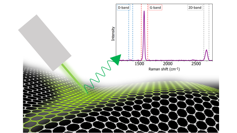
The structure and bonding of graphene make it well suited for Raman spectroscopy. Graphene is one atom thick carbon; the carbon atoms are arranged in a hexagonal lattice. The sp2 carbon bonds result in highly polarisable π bonds which give an intense Raman signal. This is because the vibrational mode is “Raman active” and this occurs when the molecular polarisability changes during the vibration. Raman spectroscopy can be used in the evaluation of graphene quality and thickness. Since Raman microscopy is non-destructive and has high spatial and spectral resolution, the technique is well-suited for gathering detailed information about the graphene film.2,3 There is also minimal or no sample preparation required for Raman spectroscopy, further adding to its ease of use and low damage risk. In this application note, an Edinburgh Instruments RM5 Raman Microscope is used to highlight how Raman microscopy an essential tool for any material scientist researching graphene.
Materials and Methods
An RM5 Raman Microscope equipped with a 532 nm laser and 1200 gr/mm grating was used to investigate three graphene samples: monolayer, bilayer, and trilayer graphene on a silicon substrate. Since graphene is an incredibly thin material, care must be taken with Raman spectroscopy to avoid laser induced heating in the sample. The RM5 has fully automated laser attenuators, controlled via the Ramacle® software, allowing the user to ensure no laser damage occurs to the sample.
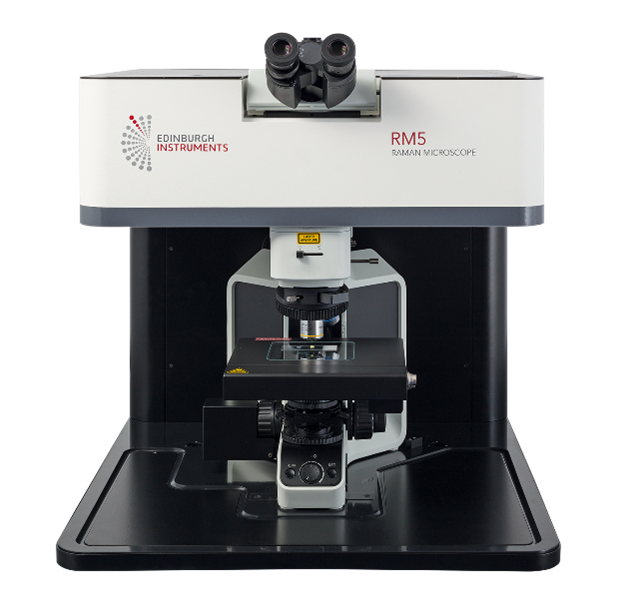
Figure 1: Edinburgh Instruments RM5 Raman Microscope
Results and Discussion
Raman Spectra of Graphene
There are 3 main bands of interest in the Raman spectra of graphene, Figure 2, the G-band, the D-band, and the 2D-band. These bands are indicative of the number of layers of graphene present and the quality of the sample. Whilst the D-band and 2D-band will always be present, the D-band will only be seen for samples containing defects. These three bands will now be discussed in detail.
The spectrum in Figure 2 was measured using a 532 nm excitation, you may also see 633 nm commonly employed. These lasers are most used due to the resonance between sample and excitation wavelength. Resonance Raman is an enhancement technique where the laser wavelength is chosen to be close to the frequency of an electronic transition in the sample. Due to the resonance properties for the main bands in Raman analysis of graphene, it is important to always use the same excitation wavelength when investigating samples to allow for comparisons to be made. The D-band and 2D-band, discussed in more detail below, will differ between excitation wavelengths, as shown in Figure 3. The difference is due to Double Resonance Raman scattering (DRR), which is a rare second-order 2-phonon process. DRR is dependent on the incoming excitation wavelength and thus the laser wavelength chosen affects peak positions. DRR is most observed in materials science, for example when studying MoS2, carbon nanotubes, and graphene.4
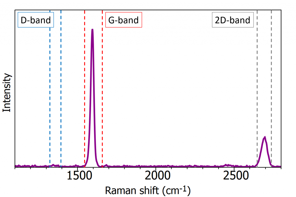
Figure 2: Raman spectrum of graphene
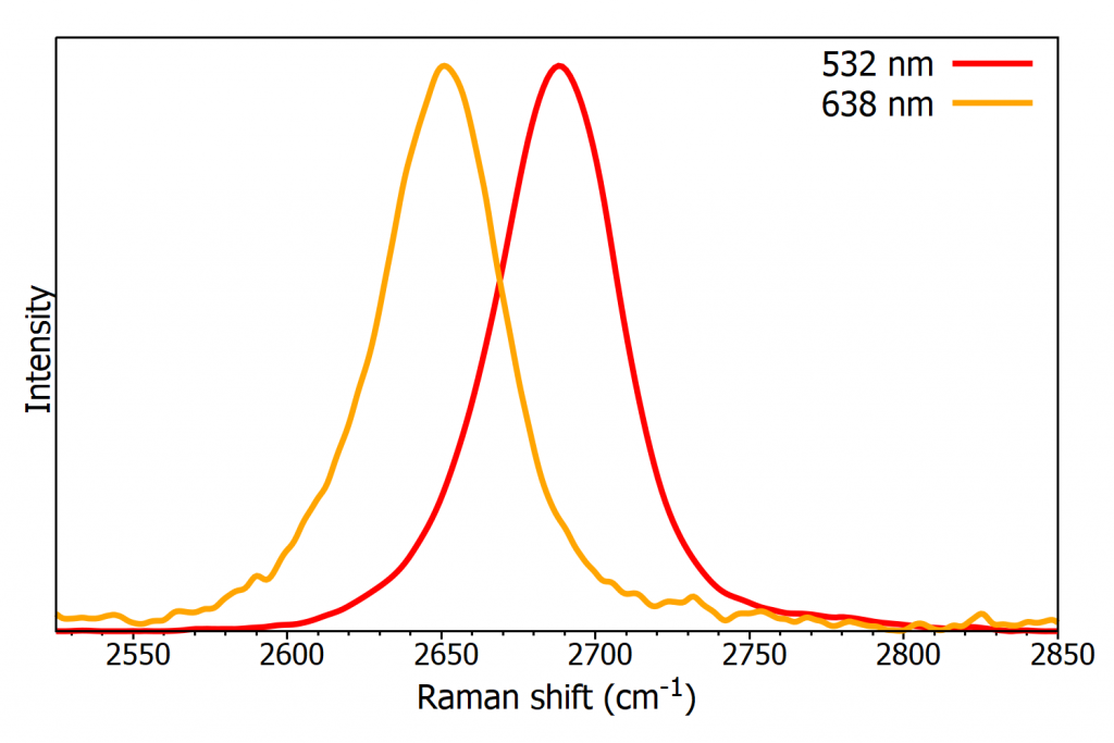
Figure 3: Normalised Raman spectra of the 2D-band from graphene excited with a 532 nm and 638 nm laser
The G-band
The G-band is a sharp band at approximately 1585 cm-1 and represents the in-plane stretching vibrations of the sp2 bonded carbon atoms. Its position is affected by the number of layers present, as shown in Figure 4, the peak shifts to lower wavenumbers as the number of graphene layers increases. This blue shift is caused by different dimer interaction as the number of layers increases. The number of layers can be calculated from the peak position using the following equation where ωG is the band position, and n the number of layers present:?
![]()
The spectra in Figure 4 also show the difference in G-band intensity between different layers of graphene, as the layers increase so too does the peak intensity, and this follows closely to a linear trend. Both changes in the G-band can be used to determine layer thickness, however the peak position is also sensitive to strain, temperature and doping so care needs to be taken when using this band for layer evaluation.
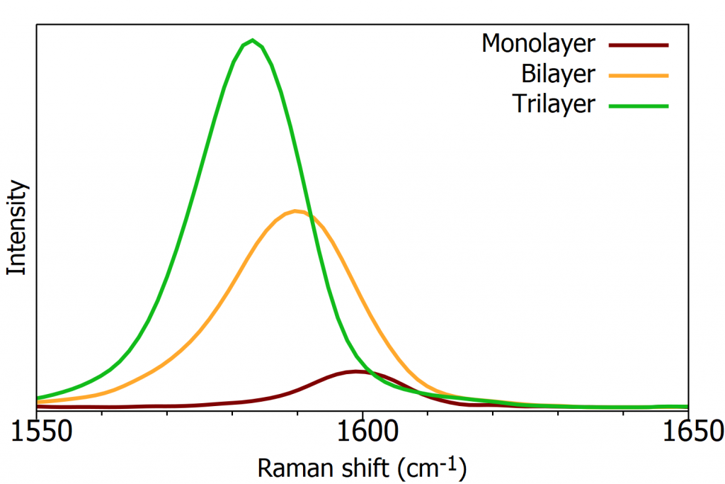
Figure 3: Raman spectra from the G-band of monolayer, bilayer, and trilayer graphene
The 2D-band
The 2D-band (also referred to as the G’-band) is also indicative of the number of layers present in the sample. The 2D-band originates from a double resonance enhanced two-phonon lateral vibrational process.6 Although this band is the second order overtone of the D-band, discussed below, it does not arise from a defect and therefore is not indicative of defects.
The 2D-band changes in shape and position as the layers of graphene increase, as shown in Figure 5. The spectra have been normalised for easier comparison. This is more complicated than a simple peak shift as seen with the G-band. Monolayer graphene has a single Lorentzian peak as there is only 1 component to the 2D-band. As the layers increase the peak broadens and changes shape. For example, the 2D-band of bilayer graphene has 4 components as there are 4 possible double resonance scattering processes, whilst there is only 1 possible for monolayer graphene. The 2D-band is also sensitive to graphene folding and this should be considered when using the band to determine layer thickness.
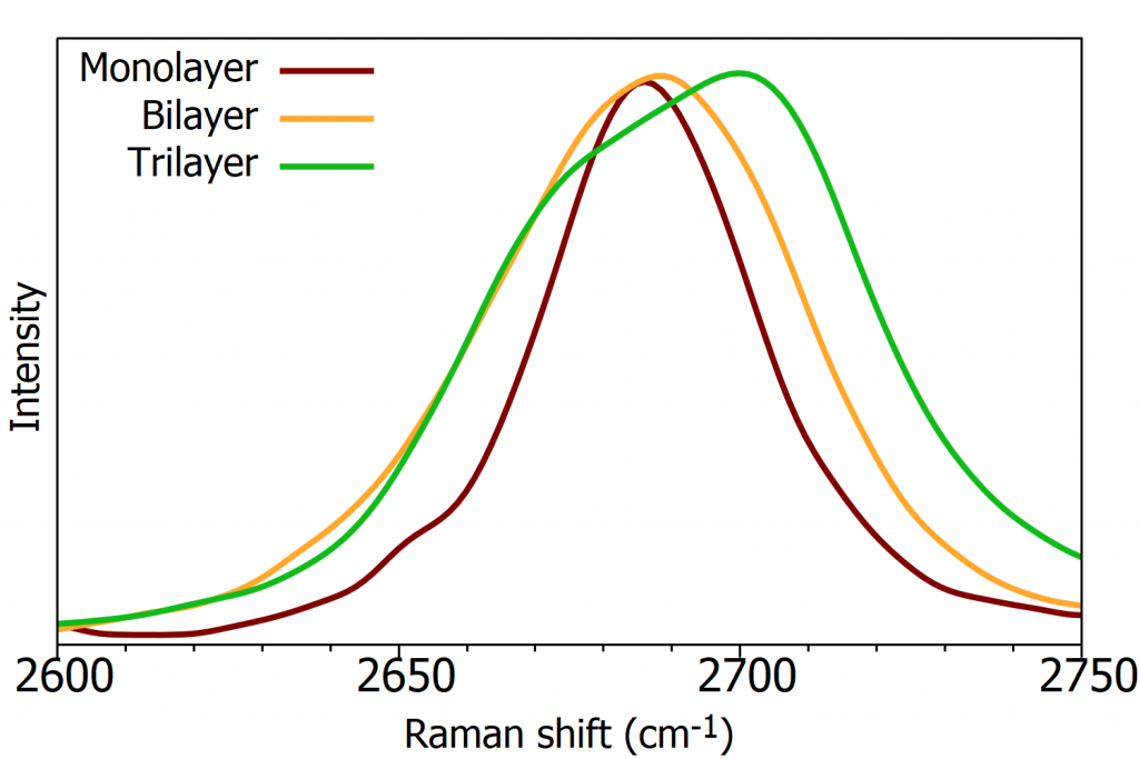
Figure 5: Normalised Raman spectra of the 2D-band of monolayer, bilayer, and trilayer graphene
The two bands discussed so far can also be used together to determine if the sample is monolayer graphene. This is by the ratio of the peak intensities. For high quality single layer graphene, the ratio of I2D/IG will be equal to 2, presented in Figure 6.
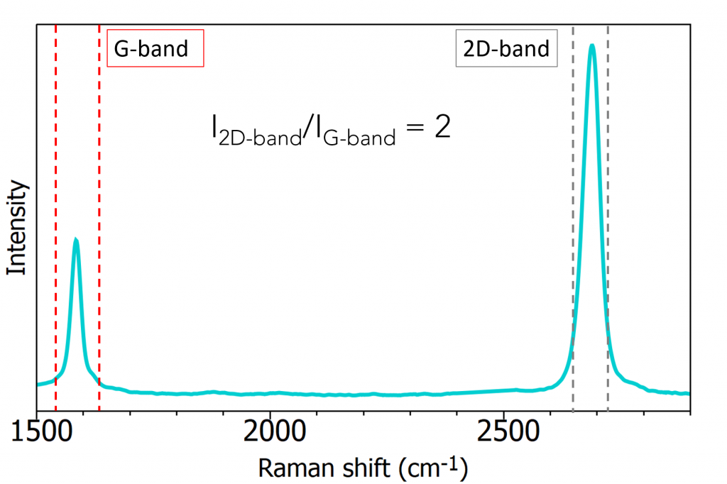
Figure 6: Single layer graphene spectrum
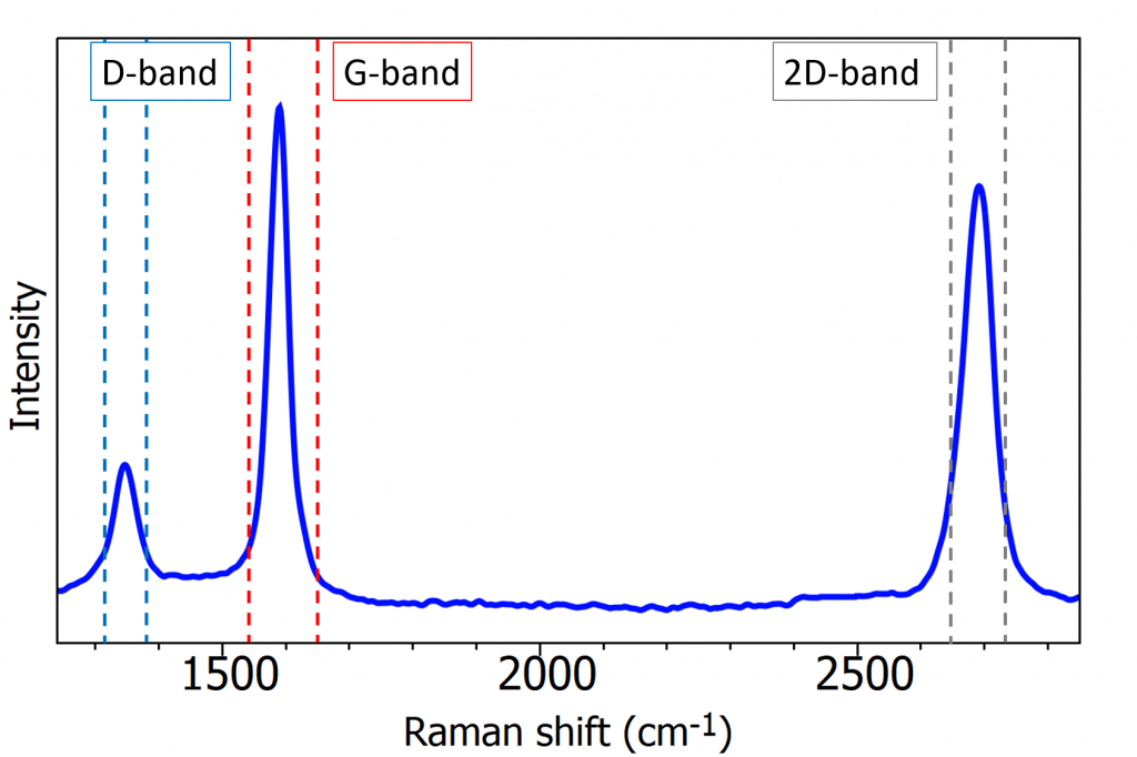
Figure 7: Raman spectrum of graphene sample containing a defect
The D-band is the peak which highlights defects in the sample, Figure 7. It can be monitored to highlight areas particularly high in defects. The more intense this band, the higher the level of disorder within the sample. It is caused by the ring breathing mode from sp2 carbon rings and must be adjacent to a defect to be Raman active. The D-band is a 1-phonon lattice vibrational process and is a double resonance band.
Raman mapping graphene samples allows the visualisation of areas particularly high in defects. The truly confocal nature of the RM5 allows for high spatial resolution which is critical for graphene analysis. Defects can include broken bonds or the presence of sp3 bonded carbon. Figure 8 a) shows the reflected white light image of a graphene sample, clearly just by this image alone it is impossible to see where the defects are located. Next a Raman map was taken using a 100x 0.9 N.A. objective with a 100 µm pinhole. From the Raman map acquired the intensity of the D-band can be plotted, producing Figure 8 b). The image shows areas of the graphene film high in defects.
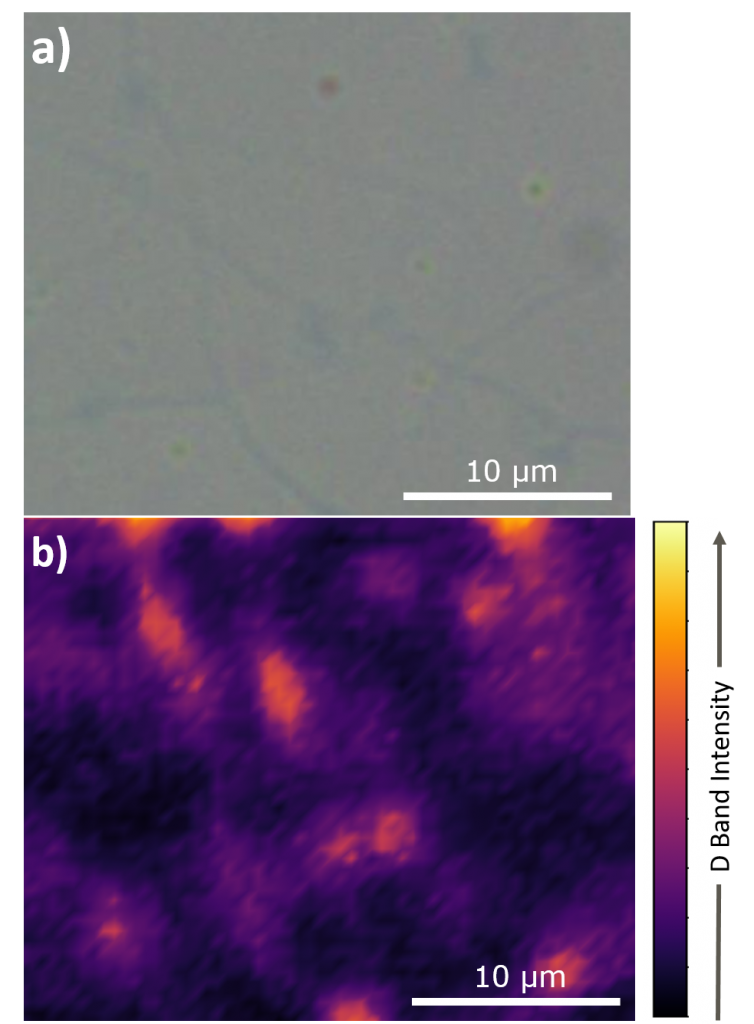
Figure 8: a) Reflected brightfield image of graphene b) Raman image highlighting areas of defects
Conclusion
In this application note the ability of confocal Raman microscopy can be used for determining the number of layers of graphene is highlighted. Additionally, we show how Raman mapping can produce images which reveal areas of the sample which are high in disorder. The RM5 Raman Microscope’s high spatial and spectral resolution allows for high quality graphene analysis, the perfect tool for any materials scientist.
References
1. Novoselov, K. S. et al. Electric Field Effect in Atomically Thin Carbon Films Supplementary. Science (80). (2004)
2. Ni, Z., Wang, Y., Yu, T. & Shen, Z. Raman spectroscopy and imaging of graphene. Nano Res. (2008)
3. Ferrari, A. C. & Basko, D. M. Raman spectroscopy as a versatile tool for studying the properties of graphene. Nature Nanotechnology (2013)
4. Wu, J. Bin, Lin, M. L., Cong, X., Liu, H. N. & Tan, P. H. Raman spectroscopy of graphene-based materials and its applications in related devices. Chemical Society Reviews (2018)
5. Wang, H., Wang, Y., Cao, X., Feng, M. & Lan, G. Vibrational properties of graphene and graphene layers. J. Raman Spectrosc. (2009)
6. Venezuela, P., Lazzeri, M. & Mauri, F. Theory of double-resonant Raman spectra in graphene: Intensity and line shape of defect-induced and two-phonon bands. Phys. Rev. B – Condens. Matter Mater. Phys. (2011)
Download Application Note
Download the complete Application Note: Raman Microscopy of Graphene
The RM5 Confocal Raman Microscope
The RM5 is a compact and fully automated Raman microscope for analytical and research purposes. The truly confocal design of the RM5 is unique to the market and offers uncompromised spectral resolution, spatial resolution, and sensitivity.
more news from Edinburgh Instruments
News Channels
- Latest News
- New Laboratory Products
- Industry News
- Laboratory Automation | IT Solutions
- Microscopy | Image Analysis
- Separation Science
- Research | Case Studies
- Video Presentations
- Events | Conferences
Subscribe to any of our newsletters for the latest on new laboratory products, industry news, case studies and much more!

Popular this Month
Top 10 most popular articles this month
Today's Picks
Looking for a Supplier?
Search by company or by product
Please note Lab Bulletin does not sell, supply any of the products featured on this website. If you have an enquiry, please use the contact form below the article or company profile and we will send your request to the supplier so that they can contact you directly.
Lab Bulletin is published by newleaf marketing communications ltd.
Media Partners