
Channels
Special Offers & Promotions
JPK Reports on the use of STM to Study Surface Plasmons in the Molecular Science Group at ISMO
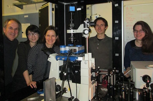
JPK Instruments, a world-leading manufacturer of nanoanalytic instrumentation for research in life sciences and soft matter, reports on how STM is being used to study surface plasmons in the Molecular Nanoscience Group at ISMO – Institut des Sciences Moléculaires d’Orsay – CNRS and the Université Paris-Sud.
One of the research goals of the Molecular Nanoscience Group at ISMO is to work towards circuits and devices in which surface plasmons (not electrons or photons) are used to transfer and manipulate information. However, why develop plasmonics when there are already solutions using electronics and photonics? Electronics has been extremely successful in the area of miniaturization, leading to computers which now fit in the palm of your hand. However, electronic devices are fundamentally limited in speed by the generation of heat. On the other hand, the use of photonics has successfully enabled fast data downloads from the Internet since optical fiber connections offer high bandwidth. Optical devices are also limited, this time in terms of size, due to the diffraction limit of light. The goal of this research group is the development of plasmonics which combines the advantages of electronics and photonics, thus producing miniaturized, high bandwidth circuits and devices which use surface plasmons. To bring this to a commercial reality, a local, low energy electrical source of surface plasmon polaritons is required.
For this research program to develop, group leader, Dr Elizabeth Boer-Duchemin takes up the story. “We propose to use an electrically biased tunnel junction as this local electrical plasmon source, and as a prototype, we consider the tunnel junction formed between the tip of a scanning tunneling microscope and a metallic sample. We chose to work with JPK for a number of reasons. First and foremost, the fact that the JPK STM is easily mounted on an inverted optical microscope (for surface plasmon detection) is essential for us. The design of the tip-assisted-optics (TAO) stage makes it easy to move both tip and sample independently. In our experiments, we use the STM to excite surface plasmons. These then radiate as photons which is the emitted light that we finally detect. I would also like to thank the engineering team at JPK who were extremely helpful in the project. This is a very unusual application and they played a vital part in the writing of specialised scripts to enable the work.”
The Group has been very active in publishing papers on this work. In 2016, these included publications such as Nanotechnology, and Optics Express.
more news from JPK instruments
News Channels
- Latest News
- New Laboratory Products
- Industry News
- Laboratory Automation | IT Solutions
- Microscopy | Image Analysis
- Separation Science
- Research | Case Studies
- Video Presentations
- Events | Conferences
Subscribe to any of our newsletters for the latest on new laboratory products, industry news, case studies and much more!

Popular this Month
Top 10 most popular articles this month
Today's Picks
Looking for a Supplier?
Search by company or by product
Please note Lab Bulletin does not sell, supply any of the products featured on this website. If you have an enquiry, please use the contact form below the article or company profile and we will send your request to the supplier so that they can contact you directly.
Lab Bulletin is published by newleaf marketing communications ltd.
Media Partners