Members Login

Channels
Special Offers & Promotions
The Karlsruhe Institute of Technology (KIT) uses the JPK NanoWizard family of AFMs for the nanoscale characterization of optical systems and devices
 JPK Instruments, a world-leading manufacturer of nanoanalytic instrumentation for research in life sciences and soft matter, reports on the work from the Light Technology Institute at the Karlsruhe Institute of Technology (KIT) in Germany where the JPK NanoWizard® family of AFMs provide the backbone for topographic and optical research activities.
![a) dark field microscopy image of gold nanoantennas; b) and c) SEM image of gold split rings antennas; d) AFM image of a gold dipole antenna. [The results were published in the Journal of Nanotechnology (Nanotechnology 20 (2009) 425203)] a) dark field microscopy image of gold nanoantennas; b) and c) SEM image of gold split rings antennas; d) AFM image of a gold dipole antenna. [The results were published in the Journal of Nanotechnology (Nanotechnology 20 (2009) 425203)]](/custom/dev_images/dark field microscopy.jpg) The generation and utilization of light is the unifying theme of research and teaching at the Light Technology Institute of the Karlsruhe Institute of Technology (KIT). Examples from the wide spectrum of light technology research projects and services from the institute include nanotechnology, visual ergonomics, materials science and system design. Like any successful enterprise, constant change is a key component of their operations and in the last ten years, the Institute has completed building modifications, added new measurement instrumentation and established new technology-intensive research areas. Major changes in focus have taken place, especially in the field of light sources.
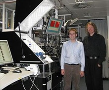
The generation and utilization of light is the unifying theme of research and teaching at the Light Technology Institute of the Karlsruhe Institute of Technology (KIT). Examples from the wide spectrum of light technology research projects and services from the institute include nanotechnology, visual ergonomics, materials science and system design. Like any successful enterprise, constant change is a key component of their operations and in the last ten years, the Institute has completed building modifications, added new measurement instrumentation and established new technology-intensive research areas. Major changes in focus have taken place, especially in the field of light sources.Dr Hans Eisler heads the DFG Heisenberg Nanoscale Science Group in Karlsruhe. It currently focuses on the development, engineering and application of quantum world based proof-of-principle devices such as single photon sources with directional emission properties at room temperature, novel energy harvesting devices comprised of resonant optical antennas, or optical antenna mediated near-field probes for microscopy and spectroscopy. The group utilizes so-called top-down nanotechnology approaches such as e-beam lithography to create functional nanodevices. Since Hans Eisler is a chemist by professional training, the DFG Heisenberg Group also uses nanochemistry to meet the requirements for bottom-up nanotechnology in the field of colloidal quantum dot research. In order to study such complex and experimentally demanding devices there is a need to correlate, whenever possible, optical information with topography information. Thus, the optical workhorse is an (inverted) epi-fluorescence microscope combined with an atomic force microscope (AFM). The optical methods include wide-field fluorescence, tip-enhanced Raman Spectroscopy (TERS), darkfield microscopy and confocal microscopy under one-photon and multi-photon excitation. The AFM triggers the topography experiments and more recently has helped to create plasmonic architectures such as resonant optical antennas via nanomanipulation schemes.
Speaking about his research goals, Eisler says, "We want to learn about the nanoscale science of matter interacting with light and vice versa to generate new ideas for future technologies based on quantum world language and principles. This includes the whole range of nanoscale fabrication and characterization."
Continuing, Eisler has positive words of praise for the JPK range of products: "Our JPK package not only includes a very nicely engineered AFM workhorse, but also has the benefit of an open software interface and an easily accessible hardware interface to combine AFM technology with other methods such as time correlated single photon counting (TCSPC). Even more importantly for us than just the naked machinery is the outstanding application and service delivered to us in a very short time frame. As we are doing research in a very competitive field, we can thus completely focus on our science and an absolutely reliable workhorse."
JPK develop, engineer and manufacture instrumentation in Germany to the world-recognized standards of German precision engineering, quality and functionality. For further details on the NanoWizard® and other products in the JPK family of nanoscale characterization systems, please contact JPK on +49 30533112070 or visit the JPK web site
Media Partners


